Twin hybrid plasma spraying of thermal barrier coatings Abstract
We developed a novel 300kW Twin Hybrid Plasma Spraying System for thermal barrier coatings. The two high power hybrid plasma torches, together with a rotatable substrate holder, enabled deposition of ZrO2-8wt%Y2O3 (8YSZ) composite coatings by utilizing each torch for thermal plasma PVD and powder spraying. Dense coating over 300ā╩m was sprayed on large Inconel substrates (50mmü~50mm) at 900oC without peeling off. Peculiar structure consisted of powder-sprayed splats and vapor-grown fine columns, layer by layer, was successfully deposited for the first time, at rates over 150ā╩m/min.In the field of thermal barrier coating (TBC) technology, two main processing methods have been adopted for decades. One is vapor deposition, which includes EB-PVD (Electron-Beam Physical Vapor Deposition), PE-CVD (Plasma Enhanced Chemical Vapor Deposition), LCVD (Laser Chemical Vapor Deposition), etc. The other is molten particle deposition, typically, APS (Atmospheric Plasma Spraying). TBCs made by the former method are characterized by columnar microstructures while splats structures are common in those deposited by APS. Due to this structural difference, the thermal and mechanical properties of such TBCs vary remarkably, as summarized in Table 1 [2-4]. The vapor deposited TBCs have the following merits: 1) Excellent strain tolerance; 2) Excellent surface finish; 3) Good erosion resistance; 4) Relative long lifetime. However, these merits are at the expense of rather high thermal conductivity and high production cost [4-7]. On the other hand, molten particle deposited TBCs demonstrate: 1) The lowest thermal conductivity; 2) High processing efficiency and low cost, but not so durable [8]. It seems that each of these two methods has its own unique strong points and shortcomings. Therefore, a new process which is able to combine all the merits would be of high interest. This research aims to develop novel composite TBCs with ultra low thermal conductivity, high strain tolerance and good affordability by a newly established high power twin hybrid plasma spraying system, which combines vapor deposition and powder spray processing together. high 250 radiation shields
Results
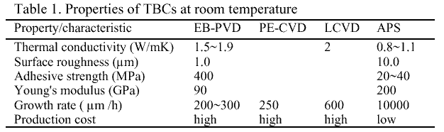
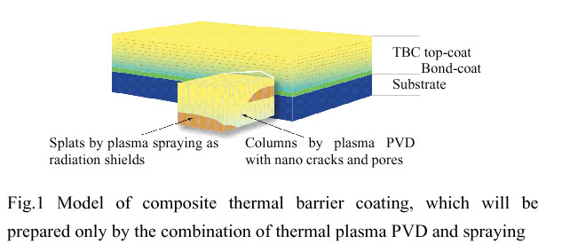
According to the theory of thermal conductivity [3,9,10], layered TBC is widely accepted as an effective structure to increase both phonon and photon scattering.At temperature over 1200oC, YSZ based TBCs was significantly transparent to thermal radiation at wavelength between 0.3~5ā╩m [11]. Therefore, a quarter wavelength filter for YSZ TBC (between ?/4 and ?) could be achieved if the layer periodicity is between 0.2~2ā╩m, which will increase the photon scattering significantly. We designed such a layered TBC system based on the combination of vapor deposited columnar structure and sprayed splats, as shown in Figure 1. In the top coat, columnar YSZ grains grow on the surface of splats layer by layer. And a dense sprayed layer near the bond-coat is preferred in order to improve oxidation resistance of the TBC system. Figure 2 (a) illustrates the schematic diagram of the novel system developed in this study. Two hybrid plasma torches, each of which is capable for plasma PVD, CVD or spraying, are positioned in a water-cooled deposition chamber. A rotatable substrate holder enables alternate exposure of substrates to the two plasma flame, and thus allows cyclic deposition by PVD, CVD and spraying, if different processes are assigned to the two hybrid torches. Each of the two torches has its own DC power supply, RF power supply and gas feeding system. And the whole system also consists of a water cooling system, a twin powder feeder and vacuum system. Figure 2 (b) shows the detailed hybrid plasma torch used here. The specifications of this twin hybrid plasma spraying system are listed in table 2.
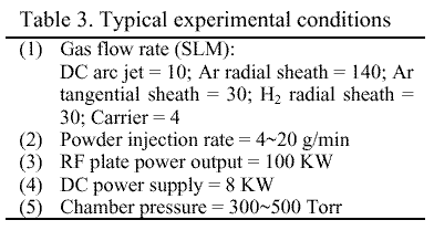
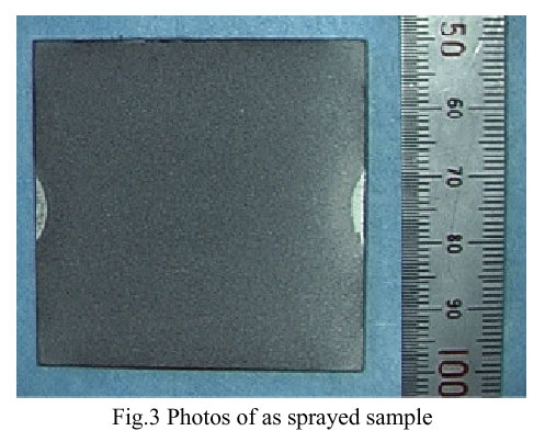
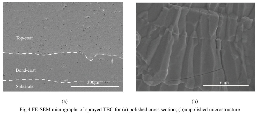
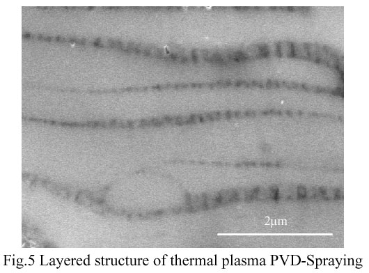
SUS304 stainless steels of 50mmü~50mmü~5mm and Inconel768 of 50mmü~50mmü~4.5mm were mainly used as substrates. Pretreatments such as sand blasting were not performed to the substrates. Commercial NiCoCrAlY powder (Starck 415.6, 44~125ā╩m, Germany) was firstly sprayed on the substrates as a bond-coat, then two kinds of 8YSZ powders (Starck 825.0, sieved, 5~12ā╩m, Germany and mechanically crushed and sieved 8YSZ, 63~88ā╩m) were deposited to form TBC top-coat by thermal plasma PVD and powder spraying when the substrate was heated up to prescribed temperature. The back-side temperature of the substrate was measured by a thermocouple. The estimated temperature gradient in the substrate is around 50K/mm, and a great temperature difference of about 250K would exist when 5mm-thickness substrates were used. Typical experimental conditions are listed in table 3. The microstructures of the prepared coatings were analyzed by field-emission scanning electron microscope (Hitachi, FE-SEM S4200). The relation between the actual applied voltages (VSi for n-type doped Si region and VBN for p-type doped cBN region) to both p- and n- type layers in heterojuncition diodes is given by ND,Si ā├ Si(Vb,Si-VSi)=NA,BN ā├ BN(Vb,BN-VBN) [13]. Here, ND,Si and NA,BN are carrier densities in both layers. Vb,Si and Vb,BN are the built-in voltages in both regions. For the heterojunction made by high doped n-Si and low doped p-BN, NA,BN ā├ BN/ND,Si ā├ Si must be much smaller than unity. In consequence, we can conclude most of the applied voltages were actually applied to the BN layers. This assumption is supported by the result that shows a drastically drop of barrier height for forwardly bias, lowering the barrier for holes that are transported by thermionic emission to silicon. On the other hand, the backward bias only causes an increase of the barrier height, and has no effects on the backward currents. Although the origin of small backward currents was not identified yet, the rectification observed in those films can be explained by this change of the barrier height for both bias conditions. From these discussions, it was suggested that heavier doping of tBN and cBN layer and decreasing the thickness of narrower band gap tBN layer were desirable for greater rectifications at high temperatures. In addition, it is important to try BN homojunctions by controlling dopant profiles.The Figure 3 shows a as-sprayed sample. The top-coat with thickness around 300ā╩m covered the whole substrate surface (50mmü~50mm) without peeling off. The white parts on both sides were under clasps used to fix the substrates. The color of the as sprayed coating was grey, indicating a slight reduction by Ar-H2 plasma. Figure 4 (a) is the FE-SEM micrograph of polished cross section, showing a dense structure without clear boundaries between the splats. The interface between top-coat and bond-coat was clean and free of cracks. Continuous growth of YSZ grains between splats was observed in unpolished cross section, as shown in Fig.4 (b), which proved strong adhesion at the splats interfaces.Figure 5 is the FE-SEM micrograph of the cross section of a peculiar layered structure deposited by both thermal plasma PVD and powder spraying. The layer periodicity was around 2ā╩m, which was in the range to act as a quarter wavelength filter, as mentioned above. The height of the columnar structures between two splats was 100~200nm, note that these grew in just one turn between the substrate rotated in and out the plasma flame, which was only about 0.04 second. This means the growth rate exceeding 150ā╩m/min was achieved, which was 30 times faster than that of ordinary EB-PVD. This is because in thermal plasma PVD, the vapor of YSZ is mainly directed to the substrate by the plasma flame, while in other vapor depositions, such as EB-PVD, the vapor disperses in the whole chamber. The diameter of the vapor grown columns was 100~200nm. Fig.5 Layered structure of thermal plasma PVD-Spraying 2ā╩m
References
[1] T. Yoshida, T. Tani, H. Nishimura, K. Akashi ü] J. Appl. Phys. 54, 640 (1983)
[2] N.P. Padture, M. Gell, E.H. Jordan ü] Science. 296, 280 (2002).
[3] J.R. Nicholls, K.J. Lawson, A. Johnstone, D.S. Rickerby ü] Surf. Coat. Technol. 151-152, 383 (2002).
[4] B. Preauchat, S. Drawin ü] Surf. Coat. Technol. 146-147, 94 (2001).
[5] T.E. Strangman, J.L. Shienle ü] J. Eng. Gas Turbines Power, 112.
[6] T.E. Strangman ü] Thin. Solid. Films 127, 93 (1985).
[7] M. Peters, K. Fritscher, G. Staniek, W.A. Kaysser, U. Schultz ü] Materialwissen. Werkstofftech. 28, 357 (1997).
[8] R.L. Jones ü] Metallurgical and Ceramic Coatings, K.H. Stern, Ed. (Champman and Hall, London, 1996), p.194.
[9] P.G. Klemens ü] R.P. Tye (Ed.), Thermal Conductivity of Solids, 1, Academic Press, London, 1969.
[10] J.E. Parrott, A.D. Stuckes ü] Thermal Conductivity in Solids, Pion Limited, 1975.
[11] J.R. Nicholls, K.J. Laswon, D.S. Rickerby, P. Morrel ü] NATO Workshop on Thermal Barrier Coatings, Aalborg, Denmark, AGARD-R-823, 1998.
(1996).